Semiconductor Electronic: Material, Devices And Simple Circuits
Notes For All Chapters Physics Class 12
1. Metals They possess very low resistivity or high conductivity.
ρ ~ 10-2.10-8 Ωm, σ ~102. 108 Sm-1
2. Semiconductors They have resistivity or conductivity intermediate to metals and insulators.
ρ ~ 10-5. 106 Ωm, σ ~ 10+5 .10-6 Sm-1
Types of Semiconductors Types of semiconductors are given below:
(i) Elements Semiconductors These semiconductors are available in natural form, e.g. silicon and germanium.
(ii) Compound Semiconductors These semiconductors are made by compounding the metals, e.g. CdS, GaAs, CdSe, InP, anthracene, polyaniline, etc.
3. Insulators They have high resistivity or low conductivity.
ρ ~ 1011 . 1019 Ωm, σ ~ 10-11. 10-19 Sm-1
4. Energy Band In a crystal due to interatomic interaction, valence electrons of one atom are shared by more than one atom in the crystal. Now, splitting of energy level takes place. The collection of these closely spaced energy levels are called an energy band.
5. Valence Band Valence band are the energy band which includes the energy levels of the valence electrons.
6. Conduction Band Conduction band is the energy band above the valence band.
7. Energy Band Gap The minimum energy required for shifting electrons from valence band to conduction band is called energy band gap (Eg ).
8. Differences between conductor, insulator and semiconductor on the basis of energy bands are given below:
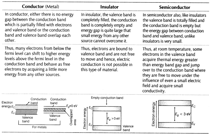
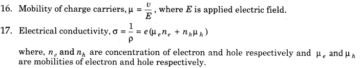
9. Fermi Energy It is the maximum possible energy possessed by free electrons of a material at absolute zero temperature (i.e. 0K)
10. On the basis of purity , semiconductors are of two types:
(i) Intrinsic Semiconductors It is a pure semiconductor without any significant dopant species present
ne = nh =ni
where , ne and nh are number densities of electrons and holes respectively and ni is called intrinsic carrier concentration.
An intrinsic semiconductor is also called an undoped semiconductor or i-type semiconductor
(ii) Extrinsic Semiconductors Pure semiconductor when doped with the impurity, it is known as extrinsic semiconductor.
Extrinsic semiconductors are basically of two types: (a) n-type semiconductors
(b) p-type semiconductors
NOTE: Both the type of semiconductors are electrically neutral.
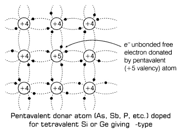
11. In n-type semiconductor, majority charge carriers are electrons and minority charge carriers are holes, i.e. ne> nh .
Here, we dope Si or Ge with a pentavalent element, then four of its electrons bond with the four silicon neighbours, while fifth remains very weakly bound to its parent atom.
Formation of n-type semiconductor is shown below:
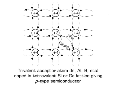
12. In p-type semiconductor, majority charge carriers are holes and minority charge carriers are eletron i.e. nh > ne .
In a p-type semiconductor, doping is done with trivalent impurity atoms, i.e. those atoms which have three valence electrons in their valence shell.
Formation of p-type semiconductor is shown below:
13. At equilibrium condition, ne nh = ni2
14. Minimum energy required to create a hole-electron pair, hv > Eg where, Eg is energy band gap.
15. Electric current, I = eA(neve + nhvh) where, A is area of cross-section.
where, ve and vh are speed of electron and hole respectively.
18. p-n Junction A p-n junction is an arrangement made by a close contact of n-type semiconductor and p-type semiconductor.
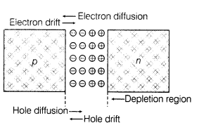
19. Formation of Depletion Region in p-n Junction During formation of p-n junction, due to the concentration gradient across p and n sides, holes diffuse from p-side to n-side (p —> n) and electrons diffuse from n-side to p-side (n —> p).
This space charge region on either side of the junction together is known as depletion region.
Depletion region is free from mobile charge carriers. Width of depletion region is of the order of 10-6 m. The potential difference developed across the depletion region is called the potential barrier.
20. Semiconductor Diode/p-n Junction Diode A semiconductor diode is basically a p-n junction with metallic contacts provided at the ends for the application of an external voltage.
![]()
The direction of arrow indicates the conventional direction of current (when the diode is under forward bias).
21. The graphical relations between voltage applied across p-n junction and current flowing through the junction are called I-V characteristics of junction diode.
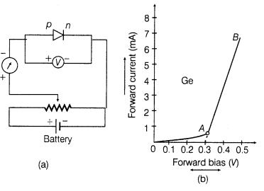
22. (i) Junction diode is said to be forward bias when the positive terminal of the external
battery is connected less to the p-side and negative terminal to the n-side of the diode. The circuit diagram and I-V characteristics of a forward biased diode is shown below:
The circuit diagram and I-V characteristics of a reverse biased diode is shown below.
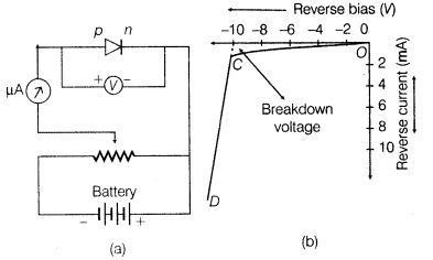
23. The DC resistance of a junction diode,
rDC = V/I
24. The dynamic resistance of junction diode,
rAC = ∆V/∆I
25. Diode as Rectifier The process of converting alternating voltage/current into direct voltage/current is called rectification. Diode is used as a rectifier for converting alternating current/voltage into direct current/voltage.
There are two ways of using a diode as a rectifier i.e.
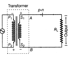
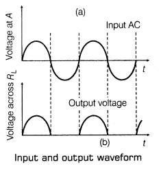
(i) Diode as a Half-Wave Rectifier Diode conducts corresponding to positive half cycle and does not conduct during negative half cycle. Hence, AC is converted by diode into unidirectional pulsating DC. This action is known as half-wave rectification.
Circuit diagram of p-n junction diode as half-wave rectifier is shown below:
The input and output wave forms have been given below:
(ii) Diode as a Full-Wave Rectifier In the full-wave rectifier, two p-n junction diodes, D1 and D2 are used. The circuit diagram or full-wave rectifier is shown below:
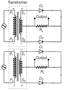
The input and output wave forms have been given below:
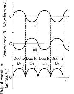
Its working based on the principle that junction diode offer very low resistance in forward bias and very high resistance in reverse bias.
26. The average value or DC value obtained from a half-wave rectifier,
![]()
27. The average value or DC value obtained from a full-wave rectifier,
![]()
28. The pulse frequency of a half-wave rectifier is equal to frequency of AC.
29. The pulse frequency of a full-wave rectifier is double to that of AC.
30. Optoelectronic Devices Semiconductor diodes in which carriers are generated by photons, i.e. photo-excitation, such devices are known as optoelectronic devices.
These are as follows:
(i) Light Emitting Diode (LED) It is a heavily doped p-n junction diode which converts electrical energy into light energy.
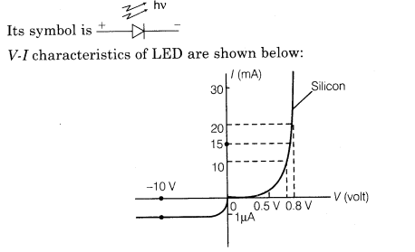
LEDs has the following advantages over conventional incandescent low power lamps
(a) Fast action and no warm up time required
(b) It is nearly monochromatic
(c) Low operational voltage and less power consumed
(d) Fast ON-OFF switching capability.
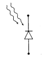
(ii) Photodiode A photodiode is a special type of junction diode used for detecting optical signals. It is a reverse biased p-n junction made from a photosensitive material. Its symbol is
Its V-I characteristics of photodiode are shown below:
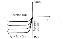
We observe from the figure that current in photodiode changes with the change in light intensity (I) when reverse bias is applied.
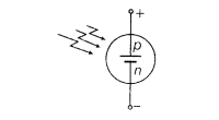
(iii) Solar Cell Solar cell is a p-n junction diode which converts solar energy into electrical energy. Its symbol is
V-I characteristics of solar cell are shown below:
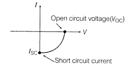
The materials used for solar cell are Si and GaAs.
31. Zener Diode Zener diode is a reverse biased heavily doped p-n junction diode. It is operated in breakdown region.
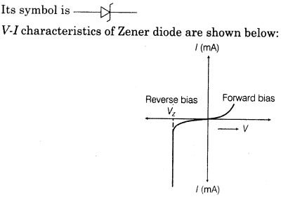
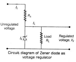
32. Zener Diode as a Voltage Regulator When the applied reverse voltage (V) reaches the breakdown voltage (Vz) of the Zener diode there is a large change in the current. So, after the breakdown voltage Vz, a large change in the current can be produced by almost insignificant change in the reverse bias voltage i.e. Zener voltage remains constant even though the current through the Zener diode varies over a wide range. The circuital arrangement is shown as follows.

Leave a Reply